based displays

A few months ago I bought "cheap" LCD PG320240WRM-HNNIS3.
Viewing area is about 80x60mm, so pixels are very small (0.22mm)
and therefore this LCD is able to display simple error difusion images too.
LCD has LED backlight and also the DC-DC voltage converter
so there is no need for external 20V as it's described in datasheet
(for contrast correction).
When I've found
that it has no controller I was very angry but I want to use it in my
project so I build this simple AVR based controller.
Recomended refresh rate is about 55-75Hz. I don't know wny but there are only 4-bit
bit data lines (drivers can work in 8-bit mode) so the controller have to be twice as fast.
The most important thing is that the controller have to send each line
in the same intevals otherwise some lines are brighter than the others.
It's very similar to CRT display driving.
I bought version with analog touchscreen so the controller also handle it.
 |
 |
Pin 1 is marked on the board.
| Pin | Name | Function |
|---|---|---|
| 1 | FLM | frame synchronization |
| 2 | M | "glass" frequency |
| 3 | CL1 | vertical clock |
| 4 | CL2 | horizontal clock |
| 5 | D-OFF | log.0 disable LCD drivers |
| 6 | DB0 | data D0 |
| 7 | DB1 | data D1 |
| 8 | DB2 | data D2 |
| 9 | DB3 | data D3 |
| 10 | Vdd | +5V supply |
| 11 | Vss | GND |
| 12 | Vee | contrast correction |
| 13 | Vss | GND |
| 14 | NC | don't connect |
| 15 | A | LED backlight A (Imax=150mA @ 3V) |
| 16 | K | LED backlight K |
CL1 and CL2 are sensitive on the falling edge (negative pulses).
When the LCD is not clocked by CL1/CL2, D-OFF have to be in log.0 otherwise
the liquid crystals are DC driven and this can dammage LCD!
When the FLM pin is log.1 then CL1 negative pulse resets vertical counter to the first line
(frame sync.). Pin M is some driver signal for the "glass" timing. It should be
200-400Hz. Some M frequencies can interferate with refresh rate, so
you have to set it experimentaly.
How to send a frame:
Set FLM to log.1, negative pulse on CL1 to reset vertical counter, FLM back to log.0.
Now send 80 4-bit words clocked by CL2. First word is placed to the left (LSB bit on the left).
After that send one negativ pulse on CL1 to increment vertical counter and wait
for the next line (always the same time). Repeat line send procedure for all lines and than again frame sync.
As I said before - you can't send all the lines in some 5ms and then doing something else for another 20ms.
You HAVE TO send lines in the same intervals. After the last one is send the first one
have to be send again in the same interval. Contrast of each individual line depends on
the CL1 period. Also all CL2 periods should be equal.
So how to do that? Lets say we have 55FPS frame rate. Than we have to send
1056000 4-bit word per second in average and much more in peak. This is not
ideal situation for the main AVR in the application because there left only
some 25% power @ 16MHz to other operations (in standard connection).
So the controller needs other MCU.
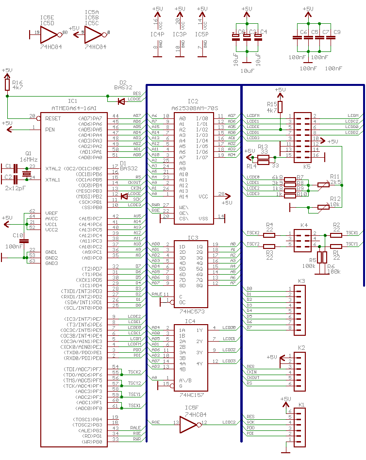
Because one image is 9600B big external SRAM in needed.
The smallest AVR with XRAM interface is ATmega64 (or ATmega128 in the same package).
It's not possible to drive CL2 pin by SW loop beacause it's very slow. So the CL2
signal is taken directly from RAM RD pin. The second very slow operations is
selecting low/high nibble from the byte for 4-bit LCD data lines so there is
external multiplexer connected directly to the XRAM data port.
It's controlled by XMEM interface A0 pin and 32kB
SRAM is connected on A1-A15 pins. It means that the LSB of XMEM address selects
low/high nibble for the LCD.
With theese two HW updates the AVR is capable
to send 2,66MB/s to the LCD at 16MHz (with no wait cycles for the external RAM).
It means 5,33M LCD words per second.
Then one line is sent in only about 280 clocks and therefore there is next more than 900 cycles
for other operations (for 55FPS refresh rate) like sending new data from master MCU to controller.
 |
Because MCU is not as busy as I thought first time I added touchscreen controler through the ADC
pins. You can read directly ADC values in X,Y or values corrected to the 320x240 resolution by
calibration values which you have to send into it. There is also implemented
digital filtering for the touchscreen with some options. You can also setup
contrast, M frequency, switching one of 3 image buffers (usefull for double buffering),
setting address in actual image buffer and some others.
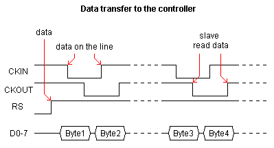
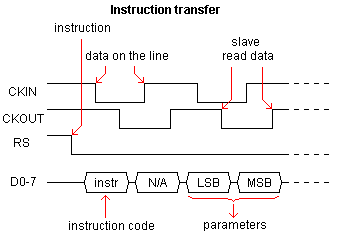
Comunication with master MCU is synchronous through 8-bit data line. Data are not transfered
with CK pulses because it was too slow. Data byte is transfered with each
edge of CK signal and controller have to acknowledge each byte transfer by second CK pin.
When data are transfered from slave to the master, CKIN/CKOUT pin functions are
switched. Check graphs for details. Used system can transfer at least 2 Bytes at the time.
It's absolutely needed to send instructions as fast as it's possible becauce
during some instructions LCD refresh (IRQ) is disabled. So disable all IRQs in tha master
MCU during instructions. Also you should never stop transfer between 2B transfer.
Instruction/data transfer is selected by RS pin just like with HD44780 controller.
RESET signal of this controller should be connected to the RESET of main MCU to protect LCD
during ISP programming.
When sending data the write address is automaticaly incremented.
Sended bytes are organized horizontaly from left to the right and from the top.
 |
 |
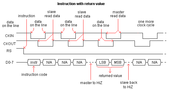 |
Table with instructions and fuse settings are in the sources.
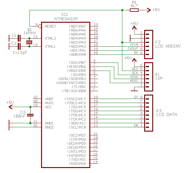
Connection to the LCD is via MLW16 connector because I haven't found the right one.
LCD pin numbers corresponding with MLW16 pin nubers.
Touchscreen is connected via MLW06 and unfurtunately there is no marking
so you have to connect 4 lines experimentaly (use ohmmeter to find the right ones).
Source and bin,
PCB 600dpi top,
PCB 600dpi bottom,
mounting plan top,
mounting plan bottom.
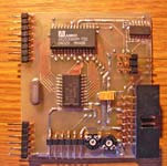 |
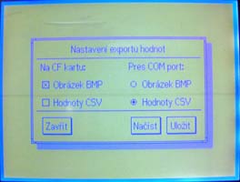
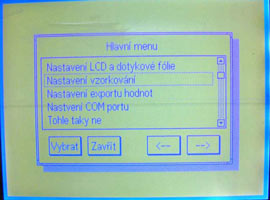
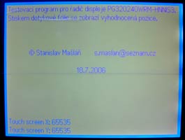
This simple application sends a few texts on the LCD in some variation Arial 10pt font and it reads the touchscreen values. If you press TS the corresponding coordinates are displayed. This MCU has only 2kB RAM - it's not possible to draw some complicated graphics.
 |
In the code you can find some bin/BCD conversion routines,
string write from the FLASH, BCD without leading zeroes write routines and some others.
There are the most important comunication routines for the LCD.
each line is generated with verticaly organized bytes because it's
much more faster with proportional texts. After the line is completed
some routine transforms it to the horizontal organized bytes.
Then the image is send on LCD.
Because of only 2kB RAM it takes some time to redraw entire image
there is simple double buffering.
Source and bin/hex.
 |
Last update: 16.12.2006
 |
 |